Fabrication of metal nanodots electrochemical deposition with ultrathin AAO as the template mask
Next-generation non-volatile memory needs fast operating speed, low power consumption, and good electrical reliability. Scaling is also very important for high-density data storage. Resistive switching random access memory (ReRAM) and the related memristors are promising candidates for next-generation non-volatile memory because of its simple metal–insulator–metal (MIM) structure and superior scalability. In addition, ReRAM has multilevel data storage capability.
In 2016, Ji-Min Song and Jang-Sik Lee reported the fabrication of resistive switching memory devices with nano-template-assisted bottom up growth. The electrochemical deposition was adopted to achieve the bottom-up growth of nickel nanodot electrodes.

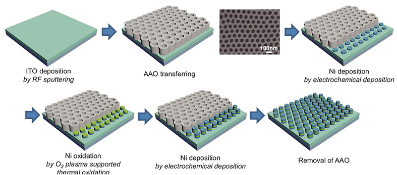
Fig. 1 Schematic procedure for nano-scale resistive switching random access memory (ReRAM) device fabrication. Planar SEM image of transferred AAO template is shown in the figure. The Ni is synthesized by electrochemical deposition with AAO as the template mask and finally array of MIM (Ni/NiO/Ni)-structured nanoscale ReRAM devices is fabricated.

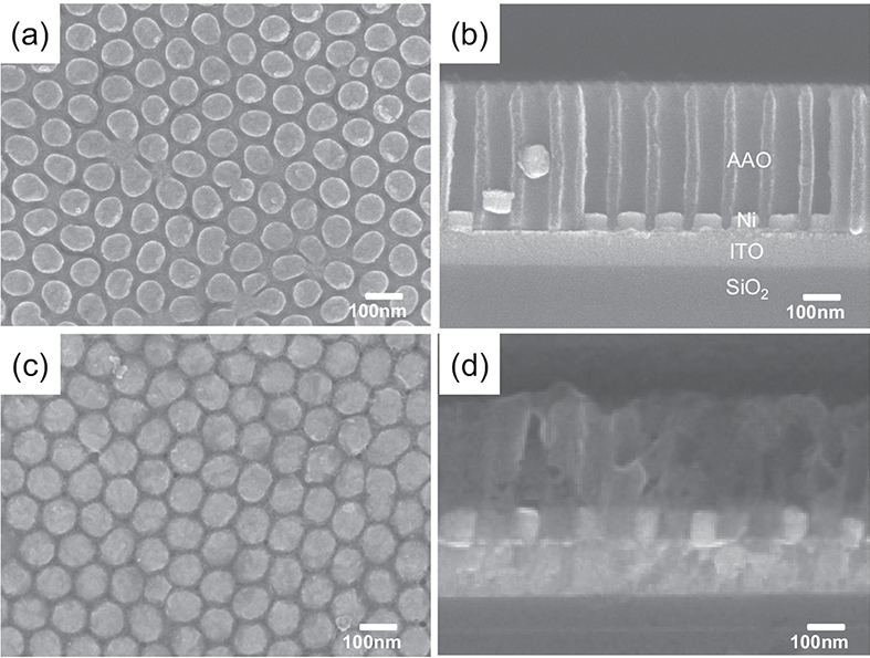
Fig. 2 (a) Planar and (b) cross-sectional SEM images of electrochemically deposited Ni nanodots. (c) Planar and (d) cross-sectional SEM images of Ni/NiO/Ni structured nanodot ReRAM devices.
Fig. 1 shows the fabrication of the Ni/NiO/Ni structured nanodot array. Indium tin oxide (ITO) deposited on SiO2 substrate was used as the working electrode for electrochemical deposition. The pore array was very well aligned with the hexagonal structure; the pore size was about 75 nm, the distance from pore to pore was about 100 nm, and the pore density was around 1x1010cm-2. As shown in Fig. 2 the AAO template had a depth of about 300~400 nm, and it grew in the direction perpendicular to the substrate. The depth of the AAO template can be easily controlled by controlling the second anodization time. As shown in Fig. 2(a,b), the Ni nanodots formed uniformly, and the pattern was well aligned with the hexagonal-packed structure as in the AAO templates. The thickness of the Ni layers that formed on the ITO layer by electrochemical deposition for 1 min was 40 nm (Fig. 2(b)).
It is difficult to implement electrodeposition by roughly putting the AAO templates onto conductive substrates due to the limited the adhesion between the AAO templates and the substrates. Vigorous electrochemical reactions may delaminate the template from conducting substrates. In Ji-Min Song and Jang-Sik Lee’s paper, there is little information about how to enhance the adhesion between the AAO templates and the substrates.

Fig. 3 Schematic diagram depicting the synthesis of highly ordered nanorod arrays fabricated directly on the conducting substrates.
In 2017, Chuanju Wang et al. reported the fabrication of highly ordered and vertically standing nanorod arrays of both metals and semiconductors on Au films and indium tin oxide glass substrates using ultrathin AAO templates. They studied how to get excellent adhesion between AAO and substrates. To improve the adhesive force between AAO templates and the conducting substrates, hydrophilic treatment was carried out to improve the wetting of the two materials. For the AAO template, it was immersed in hydrogen peroxide (30 wt %) for 2 h at room temperature to improve its hydrophilic property. Hydrophilic treatment of the Au film and ITO glass was performed using different methods to decrease the contact angle of the conducting substrates. These hydrophilic modifications resulted in strong adhesion between the AAO templates and the substrates, thus enabling the use as templates for the fabrication of nanorod arrays through electrodeposition, as shown in Fig. 3.

Fig. 4 SEM images of Ni nanorod arrays on the Au film (a) and ITO glass (b), CdSe nanorod arrays on the Au film (c), and silver nanorod arrays on the ITO glass (d). The inset of SEM showing higher magnification of the array (individual Ni nanorods in b) structure with scale bars of 200 nm.
SEM images of metal and semiconductor nanorod arrays (Ni, CdSe, Ag) on conducting substrates are shown in Fig. 4 All nanorods directly generated from the conducting substrate are ordered in length and morphology.
Electrochemical deposition is a conventional deposition method. By using this method metal deposition can be conveniently achieved with a simple solution process, but without a vacuum deposition process. Another advantage of electrochemical deposition is that the materials grow through the AAO from the bottom of the template. Because of this advantage, the nanosized mask is not obstructed with materials during deposition. Nanorod arrays can be obtained when the deposition time is long enough. In contrast, PVD methods such as sputtering are limited because nanosized masks become clogged with deposited materials. Thus, there is a limit in fabricating nanoscale devices by the PVD method.
Reference:
Sci. Rep.2016,6,18967.
Langmuir 2017, 33, 503−509.
http://www.nature.com/articles/srep18967
http://pubs.acs.org/doi/abs/10.1021/acs.langmuir.6b03999
Just a reminder: To the best of our knowledge, there are only two report on fabricating nanoparticles or nanorods using electrochemical deposition via transferred ultrathin AAO template, so this technique may be immature.
