3. Isotropic AAO templates
3.1. Fabrication of metal nanowires
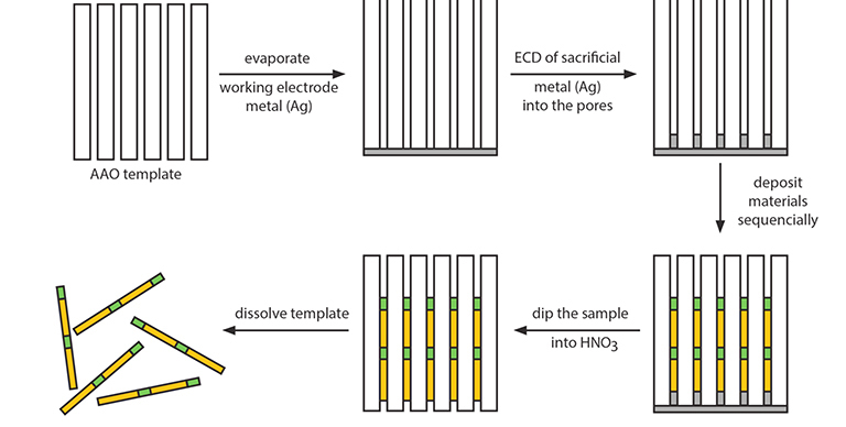
Fig. 3.1 General scheme for electrochemical deposition (ECD) of materials into porous AAO.
In general, to synthesize nanowires, the same general procedure can be applied irrespective of the materials to be deposited (Fig. 3.1). First, a thin Ag layer is deposited onto one face of an AAO membrane. This Ag layer serves as the working electrode in the deposition of desired materials. Next, a thin layer of sacrificial Ag (or Ni) is electrochemically deposited into the pores. After that, the desired material is electrochemically deposited. The resulting nanowires/AAO composite sample then is dipped into HNO3 solution to remove the Ag working electrode layer and the sacrificial layer (Ag or Ni). The nanowires can be collected by dissolving the AAO template using an appropriate AAO etchant (typically, KOH or H3PO4). The choice of oxide etchant depends on the material deposited; the etchant solution should not react with the nanowire material. The diameter of the resulting nanowires is determined by the pore size of the porous AAO template, while their length is proportional to the total amount of charge passed during the electrochemical deposition. Various metal nanowires (e.g., Au, Ag, Pt, Ni, Pb, Cu, Zn, Co, Sb) have been synthesized in porous AAO templates. These single component 1D metallic nanowires have been used as model systems for systematically investigating various research issues in chemistry and physics, for example, the catalytic, magnetic, thermoelectric, and plasmonic properties of 1D nanostructures.
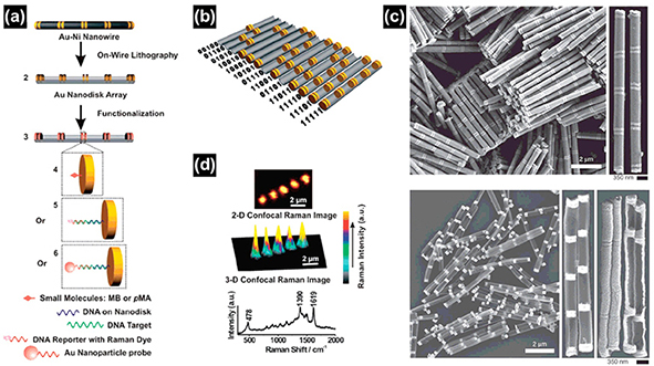
Fig. 3.2 Scheme of the nanodisk code method. (a) Synthesis and functionalization. (b) Thirteen possible 5-disk-pair nanodisk codes with the corresponding binary codes. (c) SEM images of Au/Ni multisegmented nanorods before (top) and after (bottom) deposition of the backing layer and Ni etching. (d) Two-dimensional (top) and three-dimensional (middle) scanning Raman microscopy images of a 11111 nanodisk code. Representative Raman spectrum of methylene blue (bottom) taken from the center of the hot spot generated in the middle disk pair shown in the Raman maps above.
Multisegmented metallic nanowires can conveniently be prepared by sequentially changing the electrolytic solution during the electrodeposition. Judicious control of the length of each segment allows one to obtain submicrometer barcodes, which can be used as platforms for multiplexed bioassays. The differential reflectivity of adjacent metal segments and the selective self-assembly of appropriate molecules on specific metal segments enable the identification of striping patterns by conventional optical microscopes. Thiolterminated molecules were assembled into heterometallic nanogaps (i.e., Pt/2-nm gap/Au) to observe their molecular diode behavior. The on-wire lithography (OWL) technique was further extended to develop a new encoding system by the same group. By taking advantage of the facile control of the length of segments in the nanowire, dispersible 1D objects containing arrays of nanodisks were prepared and functionalized with Raman active chromophores. This allowed encoding of individual nanodisks both physically and spectroscopically (Figure 3.2). As proof-of-concept, the authors demonstrated multiplexed DNA detection at target concentrations as low as 100 fM.
Reference:
Chem.Eur.J. 2002, 8, 4355.
Science 2001, 294, 137.
Chem. Mater. 2003, 15, 776.
Chem.Phys. Lett. 2004, 388, 406.
Adv. Mater. 2000, 12, 582.
Appl. Phys. Lett. 2005, 86, 152510.
Nano Lett. 2005, 5, 1247.
J.Magn. Magn. Mater. 2005, 290−291, 1210.
Jpn. J. Appl.Phys. 2005, 44, L469.
Mater. Lett. 2006, 60, 2069.
Adv.Mater. 2002, 14, 1227
Nano Lett. 2007, 7, 3849.
Nat. Protoc. 2009, 4, 838.
3.2. Bulk Metamaterials with Negative Refraction.
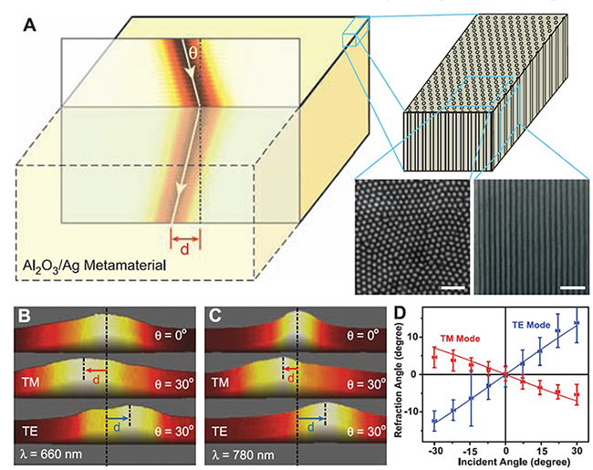
Fig. 3.3 Negative refraction in bulkmetamaterial at visible frequencies. (A) (Left) Schematic of negative refraction from air into the silver nanowire metamaterials. (Right) Nanowires embedded in an alumina matrix, as well as scanning electron microscopy images showing the top and side view of the nanowires (60-nm wire diameter and 110-nmcenter-to-center distance). The scale bars indicate 500 nm. Measured beam intensity at the existing surface of the metamaterial slab at the wavelength of 660 nm (B) and 780 nm (C). The lateral displacement (d) of TM polarized light shows the negative refraction in the metamaterial at both wavelengths, whereas TE light undergoes positive refraction. The horizontal sizes of (B) and (C) are 5 mm and 12 mm, respectively. (D) The dependence of refraction angles on incident angles and polarizations at 780-nm wavelength. The negative refraction occurs for broad incident angles. The experiment data agree well with calculations (solid curves) using the effective medium theory. The sample thicknesses in (B) and (C) are 4.5 mm and 11 mm, respectively.
In 2008, Xiang Zhang team reported observations of negative refraction in bulk metamaterials composed of silver nanowires with separation distance much smaller than the wavelength at optical frequencies (Fig. 3.3A). A porous alumina template was prepared by electrochemical anodization, into which silver nanowires were electrochemically deposited. Sample was illuminated by a collimated diode laser beam at different incident angles. The results are shown in Fig. 3.3 B and C, for incident light at wavelengths of 660 nm and 780 nm, respectively. When the incident angle is 30°, the transmitted beam is shifted to the left for transverse magnetic (TM)–polarized light, which corresponds to the negative refraction. The subwavelength composite forms an effective medium with opposite signs of electrical permittivities along and perpendicular to the wires. The hypobolic dispersion enables negative light refraction even though the phase velocity remains positive. Conversely, the transverse electric (TE)–polarized light undergoes positive refraction. Figure 3.3D shows the dependence of refraction angles on a range of incident angles at 780 nm. The group refractive indices of the metamaterial are shown to be –4.0 and 2.2 for TM and TE light, respectively.
Reference:
Science, 2008, 321, 930.
Phil. Trans. R. Soc. A, 2011, 369,3434–3446.
Optics Express, 2009, 17, 22380-22385.
PANS, 2011, 108, 11327-11331.
3.3. Fabrication of Highly Efficient, Broadband Plasmonic Absorbers for Solar Steam Generation
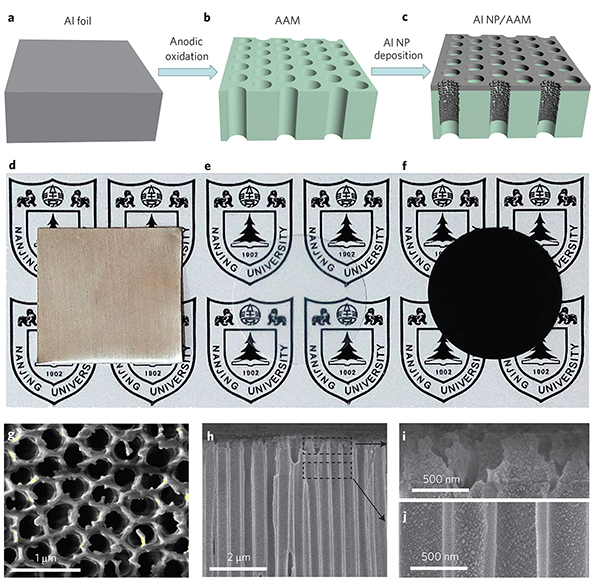
Fig. 3.4 Fabrication process and characterization of the Al NP-based plasmonic structure. (a) Aluminium foils served as the source materials for the entire fabrication process. (b) Anodic aluminium oxide membrane (AAM) fabricated by anodic oxidation. (c) The Al NP/AAM structure formed after the NP deposition. d–f, Optical photographs of the aluminium foil (d), AAM sample (e) and Al NP/AAM structure (f) observed from the AAM side. g–h, High-resolution SEM images of the structure: the top view (g) and cross-section (h). i,j, Magnified images of the areas indicated in h.
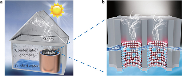
Fig. 3.5 (a) Experimental set-up for solar desalination. (b) Schematics of the plasmon-enhanced solar desalination process.
Plasmonics has generated tremendous excitement because of its unique capability to focus light into subwavelength volumes, beneficial for various applications such as light harvesting, photodetection, sensing, catalysis and so on. In 2016, Jia Zhu team demonstrateed a plasmon-enhanced solar desalination device, fabricated by the self–assembly of aluminium nanoparticles into a three-dimensional porous membrane. The formed porous plasmonic absorber can float naturally on water surface, efficiently absorb a broad solar spectrum (>96%) and focus the absorbed energy at the surface of the water to enable efficient (~90%) and effective desalination (a decrease of four orders of magnitude).
Their aluminium-based plasmonic structure (Fig. 3.4) consists of three components: the nanoporous anodic aluminium oxide membrane (AAM), close–packed aluminium NPs (along the sidewalls of the nanopores) and a thin layer of aluminium (on the top surface of the AAM). As shown in Fig. 3.4a–c, the plasmonic structures can be fabricated through a low-cost and scalable process that has two basic steps, the formation of the AAM and the self–assembly of the NPs, with aluminium as the only raw source material. Aluminium foil (Fig. 3.4a) is first used for anodic oxidation to fabricate the porous AAM. A typical porous AAM (shown in Fig. 3.4b) with nanoscale pores is transparent (Fig. 3.4e). The nanoporous AAM is then transferred into the physical vapour deposition (PVD) chamber for aluminium evaporation. During the evaporation it is expected that aluminium ions will reach the top surface of the AAM and therefore form a thin layer (Fig. 3.4c). Some of the aluminium ions also penetrate deeply into the nanopores, energetically impact the sidewall of each nanopore, collide with each other, move diffusively and then condense. Therefore, closepacked aluminium NPs self-assemble in the pores of the AAM after a short period of aluminium deposition. It is obvious that the original transparent AAM (Fig. 3.4e) is black after the deposition of the aluminium NPs (Fig. 3.4f ), a direct indication of the efficient and broadband light absorption of the as-prepared aluminium-based plasmonic structure (Fig. 3.4c, labelled Al NP/AAM).
Figure 3.5a shows the schematic of our solar desalination experimental set-up. Under solar illumination, the steady steam generated from the air–water interface will exit the structure and condense in the condensation chamber (with stainless steel as the heat dissipator). The nanopores of the AAM provide paths for efficient water supply and continuous steam flow and collection. The combination of the broadband efficient absorption, localized liquid–vapour phase change and the porous structure makes such aluminium-based plasmonic absorbers particularly suitable for the solar desalination process (see Fig. 3.5b).
Reference:
Science Advances, 2016, 2, e1501227
Nature Photonics, 2016, 10, 393–398
