Files for downloading:
>>>Introduction to the fabrication of nanoparticle arrays via ultrathin AAO template
>>>How to remove the Al base layer of AAO on Al substrate:
http://topmembranes.com/intro/AAO_on_Al_substrate.pdf
1. Typical applications of ultrathin AAO templates.
1.1. Fabrication of ferroelectric nanocapacitor arrays
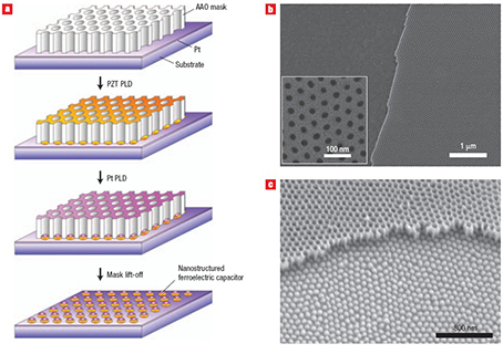
Fig. 1.1 Fabrication of ferroelectric nanocapacitor arrays via ultrathin AAO templates.
Fig.1.1 shows the pulsed laser deposition of the ferroelectric material Pb(Zr0.20Ti0.80)O3 (PZT) through an ultrathin AAO mask onto a Pt layer on a substrate, followed by the deposition of Pt and then lift-off of the mask to leave an extended array of nanocapacitors. Typical SEM micrograph of the ultrathin AAO mask and as-prepared PZT nanoisland array with the AAO mask visible at the top of the image are also shown. The nanoisland density can be estimated by assuming that the pores are arranged hexagonally. The densities are calculated to be 176 Gb inch-2 for a H2SO4-AAO mask and 68 Gb inch-2 for an H2C2O4-AAO mask.
Reference:
Nature Nanotechnology 3, 402-407 (2008).
http://www.nature.com/nnano/journal/v3/n7/full/nnano.2008.161.html
1.2 Fabrication of highly ordered arrays of metal/semiconductor core-shell nanoparticles
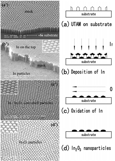
Fig. 1.2 Schematic outline of the fabrication process. (a) ultrathin AAO template on Si substrate. (b) the initial In nanoparticle arrays. (c) In/In2O3 nanoparticle arrays after the temperature ramp process. (d) the final In2O3 nanoparticle arrays.
Core-shell nanoparticles have been the subject of extensive research due to their potential application in many areas such as microelectronics, optoelectronics, catalysis, and optical devices. In 2005, Yong Lei and Wai-Kin Chim reported the fabrication of highly ordered indium oxide coated indium highly ordered indium oxide coated indium on Si substrates using a three-step oxidation process. First is the preparation of an AAO on the surface of the substrate (Fig. 1.2a). After the deposition of In (Fig. 1.2b), the AAO is removed, leaving a highly ordered In nanoparticle array on the substrate. Then, the transformation of In nanoparticles to In/In2O3 Core-shell nanoparticles and In2O3 nanoparticles was realized by a three-step oxidation process (Fig. 1.2c,d).
Reference:
Journal of the American Chemical Society 127, 1487-1492 (2005).
http://www.nature.com/nnano/journal/v3/n7/full/nnano.2008.161.html
1.3 Fabrication of the array of multiple dots.
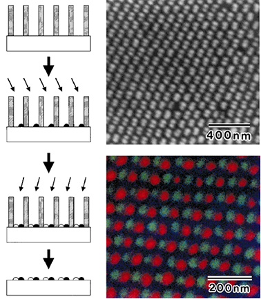
Fig. 1.3 (left) Schematic drawing of the preparation of the array of multiple dots using ultrathin AAO template. (up, right) SEM images of an array of multiple dots of Au. (bottom, right) scanning Auger microprobe image of the array of bimetallic dots of Au and Ag. The signals from Au, Ag, and Si are shown in green, red, and blue, respectively.
In Fig. 1.3, an idealized schematic of the fabrication of an array of multiple dots is shown. After the mask had been placed on the substrate, the metal was evaporated at an appropriate off normal incident angle. The appropriate angle for the spatially resolved deposition, enabled that half of the incident beam was shadowed by the wall of the holes. The second evaporation was performed by changing the incident angle of the metal beam.
Reference:
Advanced Materials 12,1031-1033 (2000).
http://onlinelibrary.wiley.com/wol1/doi/10.1002/1521-4095(200007)12:14<1031::AID-ADMA1031>3.0.CO;2-R/abstract
1.4 Fabrication of nanowire arrays.

Fig. 1.4 Schematic illustration of the proposed process to fabricate sublithographic scale VLS nanowires by using attached AAO freestanding membrane mask.
Ultrathin AAO template was carefully transferred onto the target substrate. Au catalysts were then deposited by using ion beam evaporation technique. The AAO membrane was then peeled off by a tape, remaining only as an ordered Au nanodot array. Taking the Au nanodots as catalyst, nanowire growth can be carried out by many techniques such as pulsed laser deposition (PLD) and chemical vapor deposition (CVD). Fabrication of variety nanowire arrays like MgO, ZnO, GaAs and carbon nanotube have been reported.
Reference:
RSC Advance 2, 10618–10623 (2012);Materials Letters, 154, 40–43 (2015), Applied Physics Letters 81, 5177-5179 (2002); Chemistry of Materials 16, 2757-2761(2004); Applied Physics Letters 75, 2047-2049 (1999);
http://pubs.rsc.org/en/Content/ArticleLanding/2012/RA/C2RA21643D
http://www.sciencedirect.com/science/article/pii/S0167577X15005984
http://scitation.aip.org/content/aip/journal/apl/81/27/10.1063/1.1532772
http://pubs.acs.org/doi/abs/10.1021/cm049588p
http://scitation.aip.org/content/aip/journal/apl/75/14/10.1063/1.124911
1.5 Fabrication of nanopore array or nanopillar array on substrates.
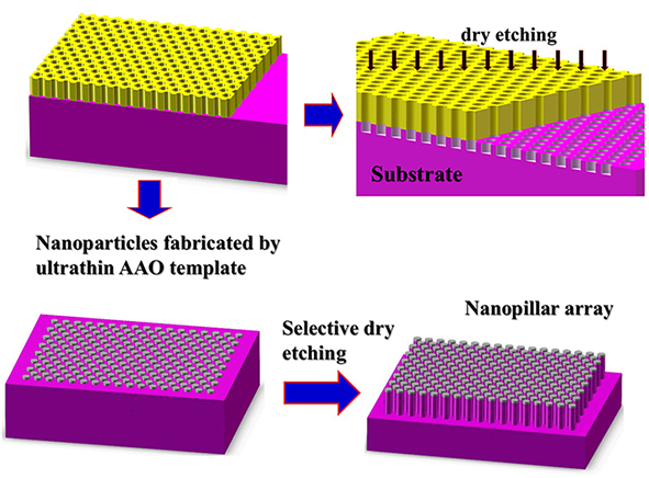
Fig. 1.5 Schematic of the fabrication of lateral two-dimensional superlattice structures: nanopore array and nanopillar array.
Through-pore ultrathin AAO template were placed on substrates such as Si, GaN and GaAs. Plasma etching were used to form nanopores on the substrate. The resultant pore diameter is about the same as the original AAO mask. The uniformity and the packing density are determined by the original AAO membranes. On the other hand, the wafer patterned with evaporated highly ordered metal nanocaps can be selective etched by plasma etching to fabricate nanopillar array.
Reference:
Journal of Applied Physics 91, 2544-2546 (2002) ;
Nano Lett., 8, 3046-3051 (2008).
http://scitation.aip.org/content/aip/journal/jap/91/4/10.1063/1.1433173
http://pubs.acs.org/doi/abs/10.1021/nl802324y
1.6 Fabrication of ordered and uniform Ag nanoparticles and their surface modification
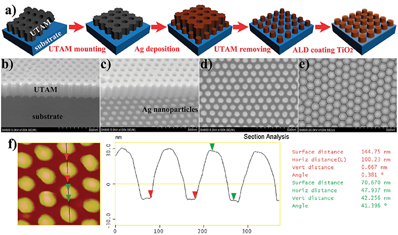
Fig. 1.6 Fabrication processes for ordered and uniform Ag@TiO2 core–shell nanocapsule structures.
In 2015, Yong Lei team reported the fabrication of ordered and uniform Ag nanoparticles and their surface modification for to enhance the Performance of Surface Plasmon Resonance for Application in Solar Energy Conversion. The fabrication processes are shown in Fig. 1.6. UTAMs with the thickness of ~300 nm were carefully mounted on ITO coated Glass substrates. Using these UTAMs as patterning masks, Ag nanoparticles were fabricated on ITO (indium tin oxide)-coated glass by electron beam evaporation. After removing the UTAM by a scotch tape, a uniform TiO2 shell layer was coated on the Ag nanoparticles by ALD to form Ag@TiO2 core–shell nanocapsule structures. By accurately controlling the dielectric TiO2 shells coated on ordered plasmonic Ag nanoparticle arrays, dipole and quadrupole SPR modes can be manipulated to coincide with each other. This finding offers a novel perspective to enhance the performance of SPR, which has important significance for its applications.
Reference:
Adv. Energy Mater. 2015, 5, 1501654.
http://onlinelibrary.wiley.com/doi/10.1002/aenm.201501654/full
1.7 Fabrication of well-ordered array of isolated epitaxial BiFeO3/CoFe2O4/SrRuO3 heterostructured nanodots
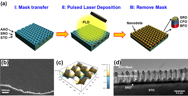
Fig. 1.7 Fabrication process and microstructures for the BiFeO3/CoFe2O4/SrRuO3 nanodot array. (a) A schematic flowchart for the fabrication procedure. (b) A top-view SEM image of the nanodot array. (c) The θ-2θ XRD diffraction pattern and (d) a reciprocal space mapping (RSM) adjacent to the STO (002) plane.
Multiferroic magnetoelectric (ME) composites exhibit sizable ME coupling at room temperature, promising applications in a wide range of novel devices. In 2016, Xiaoyan Zhang et al. explored the well-ordered array of isolated epitaxial BiFeO3/CoFe2O4/SrRuO3 heterostructured nanodots fabricated by nanoporous anodic alumina (AAO) template method. A schematic of the fabrication process is illustrated in Fig. 1.7a, which involves three steps: AAO mask transfer (i), materials deposition by PLD (ii), and mask removal (iii). The AAO mask was removed by mechanical or chemical liftoff, thus leaving the nanodot array alone. The thickness of AAO film is about 250 nm. The nanodots exhibit an average lateral size of ~70 nm and neighboring dot−dot distance of ~110 nm. It was found that the heterostructured nanodots yield apparent ME coupling, likely due to the effective transfer of interface couplings along with the substantial release of substrate clamping. These results offer good opportunities of the nanodots for applications in high-density ME devices, e.g., high density recording (>100 Gbit/in.2) or logic devices.
Reference:
ACS Nano 2016, 10, 1025−1032.
http://pubs.acs.org/doi/abs/10.1021/acsnano.5b063391.8 Fabrication of metal nanodots electrochemical deposition with ultrathin AAO as the template mask.
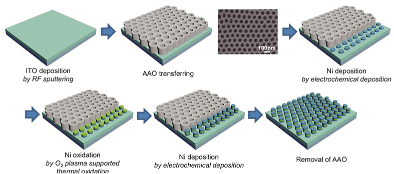
Fig. 1.8 Schematic procedure for nano-scale resistive switching random access memory (ReRAM) device fabrication. Planar SEM image of transferred AAO template is shown in the figure. The Ni is synthesized by electrochemical deposition with AAO as the template mask and finally array of MIM (Ni/NiO/Ni)-structured nanoscale ReRAM devices is fabricated.
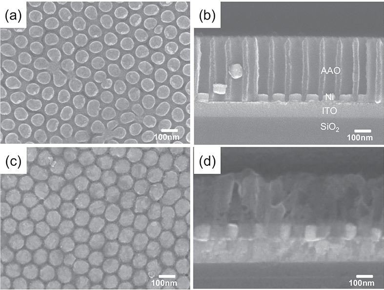
Fig. 1.9 (a) Planar and (b) cross-sectional SEM images of electrochemically deposited Ni nanodots. (c) Planar and (d) cross-sectional SEM images of Ni/NiO/Ni structured nanodot ReRAM devices.
Next-generation non-volatile memory needs fast operating speed, low power consumption, and good electrical reliability. Scaling is also very important for high-density data storage. Resistive switching random access memory (ReRAM) and the related memristors are promising candidates for next-generation non-volatile memory because of its simple metal–insulator–metal (MIM) structure and superior scalability. In addition, ReRAM has multilevel data storage capability.
In 2016, Ji-Min Song and Jang-Sik Lee reported the fabrication of resistive switching memory devices with nano-template-assisted bottom up growth. The electrochemical deposition was adopted to achieve the bottom-up growth of nickel nanodot electrodes.
Fig. 1.8 shows the fabrication of the Ni/NiO/Ni structured nanodot array. Indium tin oxide (ITO) deposited on SiO2 substrate was used as the working electrode for electrochemical deposition. The pore array was very well aligned with the hexagonal structure; the pore size was about 75 nm, the distance from pore to pore was about 100 nm, and the pore density was around 1x1010cm-2. As shown in Fig. 19 the AAO template had a depth of about 300~400 nm, and it grew in the direction perpendicular to the substrate. The depth of the AAO template can be easily controlled by controlling the second anodization time. As shown in Fig. 1.9(a,b), the Ni nanodots formed uniformly, and the pattern was well aligned with the hexagonal-packed structure as in the AAO templates. The thickness of the Ni layers that formed on the ITO layer by electrochemical deposition for 1 min was 40 nm (Fig. 1.9(b)).
It is difficult to implement electrodeposition by roughly putting the AAO templates onto conductive substrates due to the limited the adhesion between the AAO templates and the substrates. Vigorous electrochemical reactions may delaminate the template from conducting substrates. In Ji-Min Song and Jang-Sik Lee’s paper, there is little information about how to enhance the adhesion between the AAO templates and the substrates.

Fig. 1.10 Schematic diagram depicting the synthesis of highly ordered nanorod arrays fabricated directly on the conducting substrates.
In 2017, Chuanju Wang et al. reported the fabrication of highly ordered and vertically standing nanorod arrays of both metals and semiconductors on Au films and indium tin oxide glass substrates using ultrathin AAO templates. They studied how to get excellent adhesion between AAO and substrates. To improve the adhesive force between AAO templates and the conducting substrates, hydrophilic treatment was carried out to improve the wetting of the two materials. For the AAO template, it was immersed in hydrogen peroxide (30 wt %) for 2 h at room temperature to improve its hydrophilic property. Hydrophilic treatment of the Au film and ITO glass was performed using different methods to decrease the contact angle of the conducting substrates. These hydrophilic modifications resulted in strong adhesion between the AAO templates and the substrates, thus enabling the use as templates for the fabrication of nanorod arrays through electrodeposition, as shown in Fig. 1.10.

Fig. 1.11 SEM images of Ni nanorod arrays on the Au film (a) and ITO glass (b), CdSe nanorod arrays on the Au film (c), and silver nanorod arrays on the ITO glass (d). The inset of SEM showing higher magnification of the array (individual Ni nanorods in b) structure with scale bars of 200 nm.
SEM images of metal and semiconductor nanorod arrays (Ni, CdSe, Ag) on conducting substrates are shown in Fig. 1.11 All nanorods directly generated from the conducting substrate are ordered in length and morphology.
Electrochemical deposition is a conventional deposition method. By using this method metal deposition can be conveniently achieved with a simple solution process, but without a vacuum deposition process. Another advantage of electrochemical deposition is that the materials grow through the AAO from the bottom of the template. Because of this advantage, the nanosized mask is not obstructed with materials during deposition. Nanorod arrays can be obtained when the deposition time is long enough. In contrast, PVD methods such as sputtering are limited because nanosized masks become clogged with deposited materials. Thus, there is a limit in fabricating nanoscale devices by the PVD method.
Reference:
Sci. Rep.2016,6,18967.
Langmuir 2017, 33, 503−509.
http://www.nature.com/articles/srep18967
http://pubs.acs.org/doi/abs/10.1021/acs.langmuir.6b03999
Just a reminder: To the best of our knowledge, there are only two report on fabricating nanoparticles or nanorods using electrochemical deposition via transferred ultrathin AAO template, so this technique may be immature.
2. Some applications of AAO on Al substrate and V shape AAO
2.1. Fabrication of polymer nanowires or nanotubes
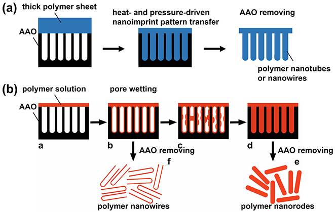
Fig. 2.1 Fabrication of polymer nanowires or nanotubes by (a) heat- and pressure-driven nanoimprint and (b) polymer solution and pore wetting.
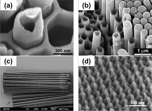
Fig. 2.3 Typical polymer nanostructures fabricated using AAO on Al substrate.
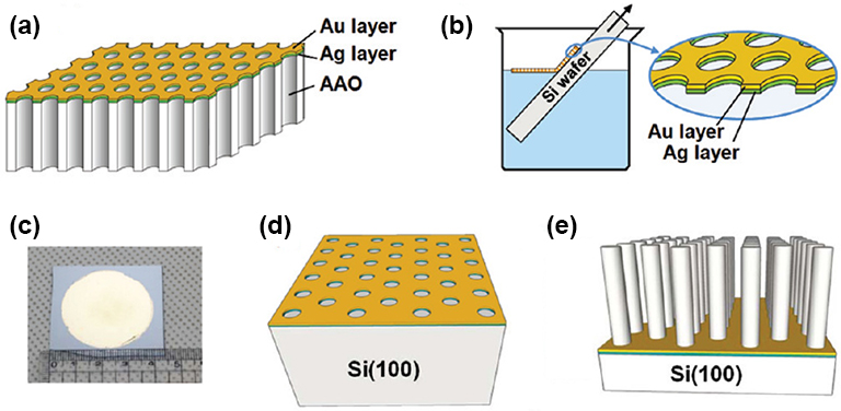
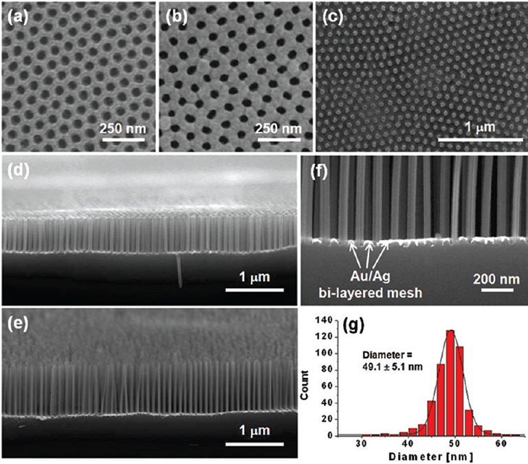
Fig. 2.4 Fabrication of Si Nanowires. (a) sequential sputter depositions of Ag and Au on the surface of AAO membrane; (b) transfer of Au/Ag bilayered metal mesh onto a silicon wafer from the surface of etching solution after removal of AAO membrane and also loosely bound metal nanoparticles from the bottom side of the metal mesh; (c) a photograph of Au/Ag bilayered metal mesh on a Si(100) wafer; (d,e) metal-assisted chemical etching (MaCE) of (100)-oriented silicon wafer for the fabrications of SiNWs.
ACS Nano, 2011, 5, 3222-3229;
ACS Nano, 2011, 5, 5242-5248;
J. Mater. Chem. C, 2013, 1, 5330.
2.4. Fabrication of Metallic Nanopore Arrays
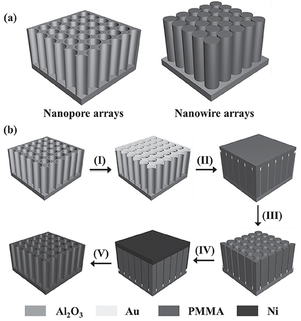
Fig. 2.6 a) Schematic structure of nanopore (left) and nanowire (right) arrays. b) Schematic illustration of the fabrication process of metallic nanopore arrays from the AAO template (Al2O3): gold layer deposition (I), polymer infi ltration (II), template removal (III), Ni electrodeposition (IV), and polymer dissolution (V).
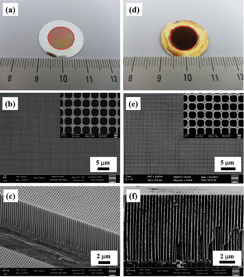 Fig. 2.7 Photographs and SEM images of the original AAO template (a–c) and of the fabricated Ni nanopore arrays (d–f). a,d) Photographs, where the area in the red circle is the nanostructured area. Scale shows lengths in centimeters. b,e) Top and c,f) cross-sectional SEM images; inset of b and e are higher-magnifi cation images.
Adv. Mater. 2014, 26, 7654–7659.
2.5. Fabrication of PDMS Flexible Nanocone Film (V shape AAO template).
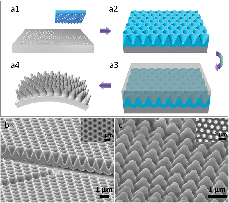
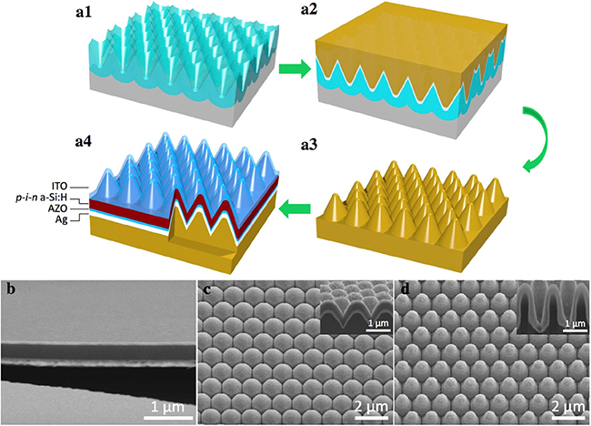
Fig. 2.8 Schematics of nanocone film and SEM images of Au-coated template and PDMS nanocone. a1) A Si mold with hexagonally ordered nanopillars used as imprint mold with four nanoimprint steps. a2) The i-cone array fabricated by a multi-step anodization and wet etching process on the imprinted Al foil. a3) Premixed PDMS poured on Au-coated template followed by a degas and curing process. a4) Regular nanocone on fl exible PDMS after peeling off. b) Aucoated template with 1 μm pitch and 1 μm depth. c) Nanocone with 1 μm pitch and 1 μm depth.
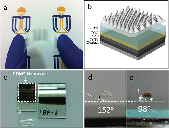
Fig. 2.9 a) Flexible nanocone fi lm. b) Schematic structure of the solar cell device with nanocone PDMS fi lm attached on the top. c) Visual effect of the nanocone AR layer on CdTe devices. The bare sample on the right and the sample with PDMS nanocone on top on the left. d) A drop of water on the nanocone PDMS film showing a large contact angle of 152°. e) A drop of water on the fl at PDMS film showing a contact angle of 98°.
Since the reflectance loss of light leads to inefficient utilization of the incident photons, various anti-reflection (AR) schemes have been developed to achieve high-efficiency solar cell devices. In 2014, Zhiyong Fan team reported utilized a facile molding process to fabricate flexible plastic AR films with three-dimensional (3D) nanocone arrays on the front surface. Fig. 2.8 a1 to a3 shows schematics of the fabrication process. Briefly, an electrochemically polished-clean Al foil was mprinted using a silicon stamp with hexagonally ordered anopillars with height of 200 nm and tunable pitch of 500 nm to 2 μm to produce a nanoindentation array on the surface of the Al foil, as shown in Fig. 2.8 a1. Thereafter, the i-cone (V shape) array (Fig. 2.8 a2) was fabricated by a multi-step anodization and wet etching process on the imprinted Al foil in an acidic solution with a proper direct-current (DC) voltage. Fig. 2.8b and the inset show scanning electron microscopy (SEM) images of a fabricated i-cone array with cross-sectional and top views, respectively. Fig.2.9a shows a photograph of a fabricated nanocone film naturally attached on a 0.18 mm thick polycarbonate film. Fig. 2.9b schematically illustrates the structure of the solar cell device with nanocone PDMS fi lm attached on the top. In addition to the AR property, it was also found that the PDMS nanocone arrays have superhydrophobic characteristic with large water contact angle.
Reference:
Adv. Mater. 2014, 26, 2805.ACS Nano, 2015, 9, 10287.
Adv. Funct. Mater. 2017, 27, 1604720
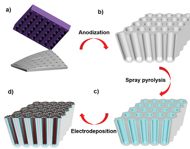
Fig. 2.10 Schematic illustration showing the fabrication process of hierarchical tubular pseudocapacitor electrodes. (a) Nanoimprint process with hexagonal nanopillar Si mold. (b) As-prepared AAO membranes after anodization and Al removal. (c) Ultrasonic spray pyrolysis (USP) deposition of FTO tubular arrays. (d) Hierarchical tubular electrodes achieved by MnO2 electrodeposition.
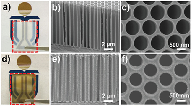
Fig. 2.11 Optical and SEM images of freestanding AAO tubular arrays with the length of 10 μm before USP (a–c). Optical and SEM images of freestanding AAO tubular arrays with the length of 10 μm after USP (d–f ).
Nanoscale, 2016, 8, 13280.
2.7 Nanostructured thin film photoelectronic device (V shape AAO template)

Reference:
Nano Energy, 2016, 22, 539
ACS Nano 2017, 11, 51133.
3. Some applications of Isotropic AAO templates
3.1. Fabrication of metal nanowires
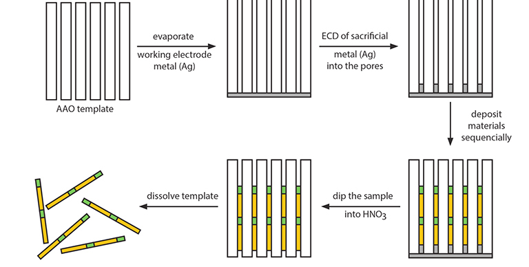
Fig. 3.1 General scheme for electrochemical deposition (ECD) of materials into porous AAO.
In general, to synthesize nanowires, the same general procedure can be applied irrespective of the materials to be deposited (Fig. 3.1). First, a thin Ag layer is deposited onto one face of an AAO membrane. This Ag layer serves as the working electrode in the deposition of desired materials. Next, a thin layer of sacrificial Ag (or Ni) is electrochemically deposited into the pores. After that, the desired material is electrochemically deposited. The resulting nanowires/AAO composite sample then is dipped into HNO3 solution to remove the Ag working electrode layer and the sacrificial layer (Ag or Ni). The nanowires can be collected by dissolving the AAO template using an appropriate AAO etchant (typically, KOH or H3PO4). The choice of oxide etchant depends on the material deposited; the etchant solution should not react with the nanowire material. The diameter of the resulting nanowires is determined by the pore size of the porous AAO template, while their length is proportional to the total amount of charge passed during the electrochemical deposition. Various metal nanowires (e.g., Au, Ag, Pt, Ni, Pb, Cu, Zn, Co, Sb) have been synthesized in porous AAO templates. These single component 1D metallic nanowires have been used as model systems for systematically investigating various research issues in chemistry and physics, for example, the catalytic, magnetic, thermoelectric, and plasmonic properties of 1D nanostructures.
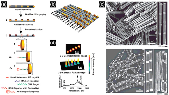
Fig. 3.2 Scheme of the nanodisk code method. (a) Synthesis and functionalization. (b) Thirteen possible 5-disk-pair nanodisk codes with the corresponding binary codes. (c) SEM images of Au/Ni multisegmented nanorods before (top) and after (bottom) deposition of the backing layer and Ni etching. (d) Two-dimensional (top) and three-dimensional (middle) scanning Raman microscopy images of a 11111 nanodisk code. Representative Raman spectrum of methylene blue (bottom) taken from the center of the hot spot generated in the middle disk pair shown in the Raman maps above.
Multisegmented metallic nanowires can conveniently be prepared by sequentially changing the electrolytic solution during the electrodeposition. Judicious control of the length of each segment allows one to obtain submicrometer barcodes, which can be used as platforms for multiplexed bioassays. The differential reflectivity of adjacent metal segments and the selective self-assembly of appropriate molecules on specific metal segments enable the identification of striping patterns by conventional optical microscopes. Thiolterminated molecules were assembled into heterometallic nanogaps (i.e., Pt/2-nm gap/Au) to observe their molecular diode behavior. The on-wire lithography (OWL) technique was further extended to develop a new encoding system by the same group. By taking advantage of the facile control of the length of segments in the nanowire, dispersible 1D objects containing arrays of nanodisks were prepared and functionalized with Raman active chromophores. This allowed encoding of individual nanodisks both physically and spectroscopically (Figure 3.2). As proof-of-concept, the authors demonstrated multiplexed DNA detection at target concentrations as low as 100 fM.
Reference:
Chem.Eur.J. 2002, 8, 4355.
Science 2001, 294, 137.
Chem. Mater. 2003, 15, 776.
Chem.Phys. Lett. 2004, 388, 406.
Adv. Mater. 2000, 12, 582.
Appl. Phys. Lett. 2005, 86, 152510.
Nano Lett. 2005, 5, 1247.
J.Magn. Magn. Mater. 2005, 290−291, 1210.
Jpn. J. Appl.Phys. 2005, 44, L469.
Mater. Lett. 2006, 60, 2069.
Adv.Mater. 2002, 14, 1227
Nano Lett. 2007, 7, 3849.
Nat. Protoc. 2009, 4, 838.
3.2. Bulk Metamaterials with Negative Refraction.
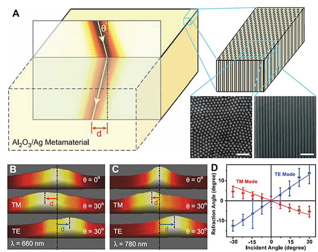
Fig. 3.3 Negative refraction in bulkmetamaterial at visible frequencies. (A) (Left) Schematic of negative refraction from air into the silver nanowire metamaterials. (Right) Nanowires embedded in an alumina matrix, as well as scanning electron microscopy images showing the top and side view of the nanowires (60-nm wire diameter and 110-nmcenter-to-center distance). The scale bars indicate 500 nm. Measured beam intensity at the existing surface of the metamaterial slab at the wavelength of 660 nm (B) and 780 nm (C). The lateral displacement (d) of TM polarized light shows the negative refraction in the metamaterial at both wavelengths, whereas TE light undergoes positive refraction. The horizontal sizes of (B) and (C) are 5 mm and 12 mm, respectively. (D) The dependence of refraction angles on incident angles and polarizations at 780-nm wavelength. The negative refraction occurs for broad incident angles. The experiment data agree well with calculations (solid curves) using the effective medium theory. The sample thicknesses in (B) and (C) are 4.5 mm and 11 mm, respectively.
In 2008, Xiang Zhang team reported observations of negative refraction in bulk metamaterials composed of silver nanowires with separation distance much smaller than the wavelength at optical frequencies (Fig. 3.3A). A porous alumina template was prepared by electrochemical anodization, into which silver nanowires were electrochemically deposited. Sample was illuminated by a collimated diode laser beam at different incident angles. The results are shown in Fig. 3.3 B and C, for incident light at wavelengths of 660 nm and 780 nm, respectively. When the incident angle is 30°, the transmitted beam is shifted to the left for transverse magnetic (TM)–polarized light, which corresponds to the negative refraction. The subwavelength composite forms an effective medium with opposite signs of electrical permittivities along and perpendicular to the wires. The hypobolic dispersion enables negative light refraction even though the phase velocity remains positive. Conversely, the transverse electric (TE)–polarized light undergoes positive refraction. Figure 3.3D shows the dependence of refraction angles on a range of incident angles at 780 nm. The group refractive indices of the metamaterial are shown to be –4.0 and 2.2 for TM and TE light, respectively.
Reference:
Science, 2008, 321, 930.
Phil. Trans. R. Soc. A, 2011, 369,3434–3446.
Optics Express, 2009, 17, 22380-22385.
PANS, 2011, 108, 11327-11331.
3.3. Fabrication of Highly Efficient, Broadband Plasmonic Absorbers for Solar Steam Generation
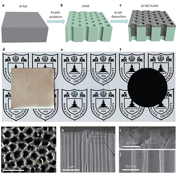
Fig. 3.4 Fabrication process and characterization of the Al NP-based plasmonic structure. (a) Aluminium foils served as the source materials for the entire fabrication process. (b) Anodic aluminium oxide membrane (AAM) fabricated by anodic oxidation. (c) The Al NP/AAM structure formed after the NP deposition. d–f, Optical photographs of the aluminium foil (d), AAM sample (e) and Al NP/AAM structure (f) observed from the AAM side. g–h, High-resolution SEM images of the structure: the top view (g) and cross-section (h). i,j, Magnified images of the areas indicated in h.
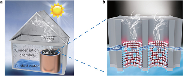
Fig. 3.5 (a) Experimental set-up for solar desalination. (b) Schematics of the plasmon-enhanced solar desalination process.
Plasmonics has generated tremendous excitement because of its unique capability to focus light into subwavelength volumes, beneficial for various applications such as light harvesting, photodetection, sensing, catalysis and so on. In 2016, Jia Zhu team demonstrateed a plasmon-enhanced solar desalination device, fabricated by the self–assembly of aluminium nanoparticles into a three-dimensional porous membrane. The formed porous plasmonic absorber can float naturally on water surface, efficiently absorb a broad solar spectrum (>96%) and focus the absorbed energy at the surface of the water to enable efficient (~90%) and effective desalination (a decrease of four orders of magnitude).
Their aluminium-based plasmonic structure (Fig. 3.4) consists of three components: the nanoporous anodic aluminium oxide membrane (AAM), close–packed aluminium NPs (along the sidewalls of the nanopores) and a thin layer of aluminium (on the top surface of the AAM). As shown in Fig. 3.4a–c, the plasmonic structures can be fabricated through a low-cost and scalable process that has two basic steps, the formation of the AAM and the self–assembly of the NPs, with aluminium as the only raw source material. Aluminium foil (Fig. 3.4a) is first used for anodic oxidation to fabricate the porous AAM. A typical porous AAM (shown in Fig. 3.4b) with nanoscale pores is transparent (Fig. 3.4e). The nanoporous AAM is then transferred into the physical vapour deposition (PVD) chamber for aluminium evaporation. During the evaporation it is expected that aluminium ions will reach the top surface of the AAM and therefore form a thin layer (Fig. 3.4c). Some of the aluminium ions also penetrate deeply into the nanopores, energetically impact the sidewall of each nanopore, collide with each other, move diffusively and then condense. Therefore, closepacked aluminium NPs self-assemble in the pores of the AAM after a short period of aluminium deposition. It is obvious that the original transparent AAM (Fig. 3.4e) is black after the deposition of the aluminium NPs (Fig. 3.4f ), a direct indication of the efficient and broadband light absorption of the as-prepared aluminium-based plasmonic structure (Fig. 3.4c, labelled Al NP/AAM).
Figure 3.5a shows the schematic of our solar desalination experimental set-up. Under solar illumination, the steady steam generated from the air–water interface will exit the structure and condense in the condensation chamber (with stainless steel as the heat dissipator). The nanopores of the AAM provide paths for efficient water supply and continuous steam flow and collection. The combination of the broadband efficient absorption, localized liquid–vapour phase change and the porous structure makes such aluminium-based plasmonic absorbers particularly suitable for the solar desalination process (see Fig. 3.5b).
Reference:
Science Advances, 2016, 2, e1501227
Nature Photonics, 2016, 10, 393–398
